C
EK-RA8D1 Kit
This topic provides board-specific information about Renesas' EK-RA8D1.
Board features
- R7FA8D1BHECBD MCU featuring ARM Cortex-M85, 2 MB Flash, 1 MB SRAM
- 4.5” 480x854 LCD Touch Display
- 64 MB SDRAM
- 64MB External Octo-SPI Flash
Supported color depths
The reference port for this board supports 16bpp color depth. See QUL_COLOR_DEPTH and Color depth for more information.
Building applications with prebuilt Qt Quick Ultralite libraries
- Open the CMake project file for the example you want to build.
- In the Configure Project window:
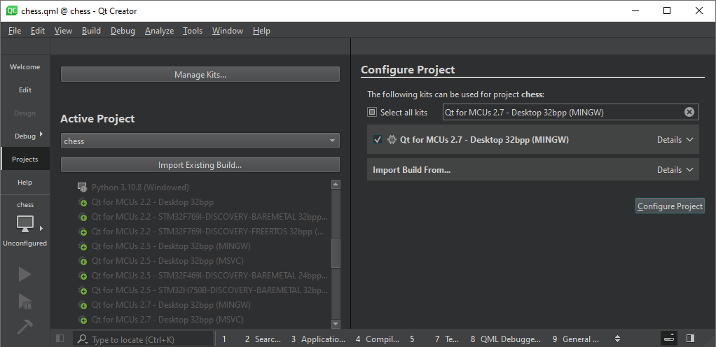
- Select the kit you created earlier. For example, Qt for MCUs 3.0.0 - Desktop 32bpp.
- Select Configure Project.
Once the project is configured, select Run or press Ctrl+r on your keyboard to build and flash the binary to the target.
Reading debug messages
By default, log data is redirected to JLink CDC UART Port (USB COM port).
Port settings
| Setting | Value |
|---|---|
| Bits per second | 115200 |
| Data bits | 8 |
| Parity | None |
| Stop bits | 1 |
| Flow control | None |
Debugging
Renesas e2 studio
Renesas e2 studio lets you debug a project using a custom configuration.
- Create a Bare Metal - Minimal project for EK-RA8D1.
- Build the project.
- Copy the Qt Quick Ultralite .elf file into the Debug folder of the e2 studio project.
- Take a copy of the original .sbd file and rename it with same name as the Qt Quick Ultralite .elf file.
- Select Run from the top menu.
- Select Debug Configurations....
- Select Renesas GDB Hardware Debugging.
- Set the Qt Quick Ultralite .elf to the C/C++ Application:.
- Select Apply and Close.
- Select Launch in 'Debug' mode.
Default FSP Configuration in Renesas e2 studio
You can find the FSP configuration .xml file used to generate the configuration below at platform/boards/renesas/ek-ra8d1-common/3rdparty/e2_project/configuration.xml.
Note: Use the default value for the property if not specified in the table.
BSP
| Property | Value |
|---|---|
| RA Common > Main stack size (bytes) | 65536 |
| RA Common > Heap size (bytes) | 262144 |
Clocks
| Clock setting | Value |
|---|---|
| SCICLK Src | PLL1P |
| PLL2 Src | XTAL |
| PLL2 Mul | x40.0 |
| LCDCLK Src | PLL2P |
| OCTASPICLK Src | PLL2P |
Note: SCICLK should be 120MHz
Note: LCDCLK should be 200MHz
Note: OCTASPICLK should be 100MHz
Stacks
Add the following stacks and configure them:
Analog > ADC (r_adc)
| Property | Value |
|---|---|
| Module > General > Name | g_adc0 |
| Module > Input > Channel Scan Mask > Channel 2 | Selected |
| Pins > AN02 | P006 |
Connectivity > I2C Master (r_iic_master)
| Property | Value |
|---|---|
| Module > Name | g_i2c_touch |
| Module > Channel | 1 |
| Module > Rate | Standard |
| Module > Rise Time (ns) | 120 |
| Module > Fall Time (ns) | 120 |
| Module > Duty Cycle (%) | 50 |
| Module > Slave Address | 0x00 |
| Module > Address Mode | 7-bit |
| Module > Timeout Mode | Short Mode |
| Module > Callback | touch_i2c_callback |
| Module > Interrupt Priority Level | Priority 6 |
| Pins > SCL1 | P512 |
| Pins > SDA1 | P511 |
Connectivity > UART (r_sci_b_uart)
| Property | Value |
|---|---|
| Module > General > Name | g_uart0 |
| Module > General > Channel | 9 |
| Module > General > Data Bits | 8bits |
| Module > General > Parity | None |
| Module > General > Stop Bits | 1bit |
| Module > Interrupts > Callback | user_uart_callback |
| Pins > RXD9 | PA15 |
| Pins > TXD9 | PA14 |
Graphics > D/AVE 2D Port Interface (r_drw)
| Property | Value |
|---|---|
| Common > Allow Indirect Mode | Enabled |
| Common > Memory Allocation | Custom |
| Module D/AVE 2D Port Interface (r_drw) > D2 Device Handle Name | d2_handle0 |
| Module D/AVE 2D Port Interface (r_drw) > DRW Interrupt Priority | Priority 2 |
Graphics > Graphics LCD (r_glcdc)
| Property | Value |
|---|---|
| Module > General > Name | g_display0 |
| Module > Interrupts > Callback Function | glcdc_callback |
| Module > Interrupts > Line Detect Interrupt Priority | Priority 12 |
| Module > Input > Graphics Layer 1 > General > Horizontal size | 480 |
| Module > Input > Graphics Layer 1 > General > Vertical size | 854 |
| Module > Input > Graphics Layer 1 > Framebuffer > Number of framebuffers | 2 |
| Module > Input > Graphics Layer 1 > Framebuffer > Section for framebuffer allocation | .sdram |
| Module > Output > Timing > Horizontal total cycles | 559 |
| Module > Output > Timing > Horizontal active video cycles | 480 |
| Module > Output > Timing > Horizontal back porch cycles | 5 |
| Module > Output > Timing > Horizontal sync signal cycles | 2 |
| Module > Output > Timing > Horizontal sync signal polarity | Low active |
| Module > Output > Timing > Vertical total lines | 894 |
| Module > Output > Timing > Vertical active video lines | 954 |
| Module > Output > Timing > Vertical back porch lines | 20 |
| Module > Output > Timing > Vertical sync signal cycles | 3 |
| Module > Output > Timing > Vertical sync signal polarity | Low active |
| Module > Output > Timing > Data Enable Signal Polarity | High active |
| Module > Output > Timing > Sync edge | Falling edge |
| Module > Output > Format > Color format | 24bits RGB888 |
| Module > TCON > Hsync pin select | LCD_TCON1 |
| Module > TCON > Vsync pin select | LCD_TCON0 |
| Module > TCON > Panel clock division ratio | 1/8 |
MIPI Display (r_mipi_dsi)
| Property | Value |
|---|---|
| Module > General > Name | g_display0 |
| Module > Low Power > Ultra Low Power State Wakeup Period | 290 |
MIPI Physical Layer (r_mipi_phy)
| Property | Value |
|---|---|
| Module > DSI PLL Frequency | 560 |
Input > External IRQ (r_icu)
| Property | Value |
|---|---|
| Module > Name | g_touch_irq |
| Module > Channel | 3 |
| Module > Trigger | Falling |
| Module > Digital Filtering | Enabled |
| Module > Digital Filtering Sample Clock | PCLK / 64 |
| Module > Callback | touch_irq_cb |
| Module > Pin Interrupt Priority | Priority 5 |
Note: Ensure that the mode of pin P510 is Output mode (Initial Low). The mode is changed to Input mode during the GT911 initialization process.
Storage > OSPI Flash (r_ospi_b)
| Property | Value |
|---|---|
| Common > Memory-mapping Support > Prefetch Function | Enable |
| Common > Memory-mapping Support > Combination Function | 64 Byte |
| Common > Memory-mapping Support > XiP Support | Disable |
| Common > DMAC Support | Enable |
| Common > Autocalibration Support | Enable |
| Common > DOTF Support | Disable |
| Module > General > Name | g_ospi_b |
| Module > General > Channel | 1 |
| Module > General > Initial Protocol Mode | SPI (1S-1S-1S) |
| Module > General > Initial Address Bytes | 4 |
| Module > General > Write Status Bit | 0 |
| Module > General > Write Enable Bit | 1 |
| Module > General > Sector Erase Size | 4096 |
| Module > General > Block Erase Size | 262144 |
| Module > General > Command Set Table | (empty) |
| Module > General > Command Set Table Length | 0 |
| Module > Defaults > Command Definitions > Page Program Command | 0x12 |
| Module > Defaults > Command Definitions > Read Command | 0x0B |
| Module > Defaults > Command Definitions > Write Enable Command | 0x06 |
| Module > Defaults > Command Definitions > Status Command | 0x05 |
| Module > Defaults > Erase Command Definitions > Sector Erase Command | 0x2121 |
| Module > Defaults > Erase Command Definitions > Block Erase Command | 0xDCDC |
| Module > Defaults > Erase Command Definitions > Chip Erase Command | 0x6060 |
| Module > Defaults > Dummy Cycles > Memory Read Dummy Cycles | 3 |
| Module > Defaults > Dummy Cycles > Status Read Dummy Cycles | 0 |
| Module > High-speed Mode > Auto-Calibration > Data latching delay | 0 |
| Module > High-speed Mode > Auto-Calibration > Auto-Calibration Address | 0x90002000 |
| Module > High-speed Mode > Command Definitions > Page Program Command | 0x1212 |
| Module > High-speed Mode > Command Definitions > Dual Read Command | 0xEEEE |
| Module > High-speed Mode > Command Definitions > Write Enable Command | 0x0606 |
| Module > High-speed Mode > Command Definitions > Status Command | 0x0505 |
| Module > High-speed Mode > Command Definitions > Sector Erase Command | 0x2121 |
| Module > High-speed Mode > Command Definitions > Block Erase Command | 0xDCDC |
| Module > High-speed Mode > Command Definitions > Chip Erase Command | 0x6060 |
| Module > High-speed Mode > Protocol | Dual data rate OPI (8D-8D-8D) |
| Module > High-speed Mode > Command Length Bytes | 2 |
| Module > High-speed Mode > Memory Read Dummy Cycles | 10 |
| Module > High-speed Mode > Status Read Dummy Cycles | 4 |
| Module > Chip Select Timing Setting > Command Interval | 2 |
| Module > Chip Select Timing Setting > Pull-up Timing | No Extension |
| Module > Chip Select Timing Setting > Pull-down Timing | No Extension |
| Pins > OM_CS1 | P104 |
| Pins > OM_DQS | P801 |
| Pins > OM_ECSINT1 | P105 |
| Pins > OM_RESET | P106 |
| Pins > OM_SCLK | P808 |
| Pins > OM_SIO0 | P100 |
| Pins > OM_SIO1 | P803 |
| Pins > OM_SIO2 | P103 |
| Pins > OM_SIO3 | P101 |
| Pins > OM_SIO4 | P102 |
| Pins > OM_SIO5 | P800 |
| Pins > OM_SIO6 | P802 |
| Pins > OM_SIO7 | P804 |
Timers > Timer, General PWM (r_gpt)
| Property | Value |
|---|---|
| Common > Pin Output Support | Enabled |
| Module > General > Name | g_timer_for_qul_tick |
| Module > General > Channel | 0 |
| Module > General > Mode | Periodic |
| Module > General > Period | 1000 |
| Module > General > Period Unit | Microseconds |
| Module > Output > GTIOCA Output Enabled | False |
| Module > Output > GTIOCB Output Enabled | False |
| Module > Interrupts > Callback | qul_tick_interrupt_cb |
| Module > Interrupts > Overflow/Crest Interrupt Priority | Priority 2 |
| Module > Interrupts > Capture A Interrupt Priority | Disabled |
| Module > Interrupts > Capture B Interrupt Priority | Disabled |
| Module > Interrupts > Underflow/Trough Interrupt Priority | Disabled |
Timers > Timer, General PWM (r_gpt)
| Property | Value |
|---|---|
| Common > Pin Output Support | Enabled |
| Module > General > Name | g_timer_PWM |
| Module > General > Channel | 7 |
| Module > General > Mode | Saw-wave PWM |
| Module > General > Period | 10 |
| Module > General > Period Unit | Milliseconds |
| Module > Output > Duty Cycle Percent | 75 |
| Module > Output > GTIOCB Output Enabled | True |
| Pins > GTIOCB | P404 |
Note: When setting the GTIOCB pin, ensure that the Operation Mode of the GPT Timer is GTIOCA or GTIOCB, and pin P404 is in Peripheral mode.
Resource storage section
By default, the application's image resource data is stored in internal flash memory. However, you can choose to store the resource data in external flash memory. Configure the ImageFiles.MCU.resourceStorageSection QmlProject property with QulResourceDataInExternalFlash when adding resources to the application using ImageFiles.files.
In a similar way, the font resource data is, by default, also stored in internal flash memory. You can choose to store the font resource data in external flash memory by using MCU.Config.fontFilesStorageSection QmlProject property with QulFontResourceDataInExternalFlash.
Available under certain Qt licenses.
Find out more.
